Basic Research
The Power to Decode Gravitational Waves Can Shape the Society of Tomorrow
Faculty of Design and Data Science / Advanced Research Laboratories ProfessorTAKAHASHI Hirotaka

Microactuator
All English text on this page has been translated automatically. Some sentences may be unnatural.
When you tilt a smartphone, the screen orientation changes. You move a controller to enjoy games with friends and family. A car senses the impact of a collision and activates its airbags. By reading the subtle vibrations of roads, bridges, and buildings, it is even possible to detect signs of deterioration that cannot be seen with the naked eye. Behind our everyday lives are countless machines that operate with extraordinary precision in a tiny world measured in micrometers. This field is known as MEMS, or Micro Electro Mechanical Systems, and is also called micromachines in Japanese. Specially Appointed Professor Hiroyuki Fujita of the Micronano Systems Laboratory at the Research Institute has expanded semiconductor microfabrication technologies into mechanical systems, opening new horizons in optics, energy, medicine, and biotechnology.
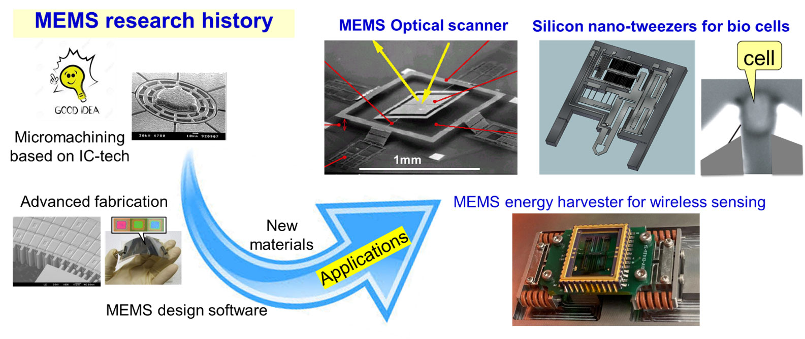
When people hear the phrase “tiny machines,” they may imagine intricate miniature craftworks. But the MEMS that Specially Appointed Professor Fujita works on are not one-of-a-kind miniatures. By applying semiconductor processing technologies, which can fabricate vast numbers of transistors at once, it becomes possible to mass-produce three-dimensional structures such as beams, gears, mirrors, and tweezers on the micrometer scale. “It would be extremely difficult if we had to carve them one by one, but by using semiconductor technology, we can make one million or even tens of millions at once. What makes it fascinating is that three-dimensional moving objects can be mass-produced in the same way as silicon chips.”
One of the studies Specially Appointed Professor Fujita worked on in the 1980s was the development of microscopic actuators that move up and down like biological cilia. Many small structures, each about 500 micrometers long, 100 micrometers wide, and 10 micrometers thick, were arranged in rows and moved by using differences in how materials expand with temperature changes. By shifting the phase of their motion little by little, they could gradually transport a silicon chip placed on top. In an electrostatic micromotor only a few millimeters in diameter, voltage is applied across a gap of just a few micrometers, generating rotational motion through electrostatic force. Large machines use magnets and coils, but in the microscopic world, static electricity becomes powerful. “Even if someone asked us to wind a one-micrometer coil, that would be extremely difficult. The smaller things become, the more useful electrostatic force becomes.”
One representative application of MEMS is the micromirror, which manipulates light. A mirror fabricated on a silicon substrate is tilted by electrostatic force to scan laser light. Moving it along one axis draws a line, while moving it along two axes draws a surface. Combined with red, green, and blue lasers, this technology can even make possible a display small enough to fit in the palm of your hand. The same principle is also involved in LiDAR, a sensor attracting attention in self-driving cars. LiDAR works by emitting laser light and measuring the distance to people or obstacles ahead from the light reflected back. If the mirror that steers the light can be made smaller, the entire device can also be miniaturized. In recent years, LiDAR has begun to be installed in smartphones as well. Technologies for controlling light are not limited to displays and automobiles. In data centers, they can also be applied to optical switches that change the paths of optical fibers connecting computers. If the direction of light can be changed without converting it into electrical signals, power consumption can be reduced and communication flexibility can be improved.
Another area Specially Appointed Professor Fujita has focused on is vibration energy harvesting, which generates electricity from faint environmental vibrations. In the age of IoT, or the Internet of Things, sensors are expected to be installed everywhere, including bridges, factory equipment, logistics systems, medical settings, and sports environments, so that conditions can be continuously monitored. However, when large numbers of sensors are deployed, battery replacement and power wiring become major challenges. This is why Fujita turned his attention to the tiny vibrations emitted by machines and structures. For example, even attaching a power-generating device to a vending machine in the city, where people hardly notice any vibration, can extract enough energy to light an LED. MEMS structures are also used in this vibration energy harvesting device. A small weight moves in response to vibration, causing a comb-shaped structure fabricated beneath it to move. The vibration creates an electrical imbalance, and current is extracted from the resulting change. Attached to equipment that vibrates continuously, such as a factory pump, the device can supply power to operate wireless sensors. It can also be installed on bridges and tunnels to detect deterioration early, or used to record the temperature and shocks experienced by cargo in transit. It is even possible to attach it behind an athlete’s ear to quantitatively measure impacts to the head. Tiny power-generating elements are becoming a foundation for sensing systems that are no longer constrained by batteries.
The scale of MEMS is also well suited to the world of cells. Cells are roughly 10 micrometers in size. Specially Appointed Professor Fujita and his colleagues fabricated microscopic tweezers for grasping cells on a chip about five millimeters square. The gap at the tip of the tweezers is about 20 micrometers. The device captures cells flowing through a microchannel and compresses them to measure their stiffness and viscosity. One possible application is evaluating the malignancy of cancer cells. For cancer to metastasize, cells must pass through tissues in the body, penetrate blood vessel walls, enter the bloodstream, and move to another location. Highly malignant cells tend to be soft, making it easier for them to pass through gaps in tissue. If cancer cells circulating in the blood can be collected and analyzed not only by number but also by their properties, the results may be useful for postoperative monitoring and prognosis. Current testing methods known as liquid biopsy mainly examine how many cancer cells are contained in blood or bodily fluids. Fujita’s goal, however, is to measure the condition of the cells themselves. These microscopic tweezers aim to convert the invisible tactile properties of cells into numerical data, providing medicine with new information for decision-making. “We want to make it possible to look not only at the number of cells, but also at the properties of the cells themselves, so we can determine whether they are truly harmful.”
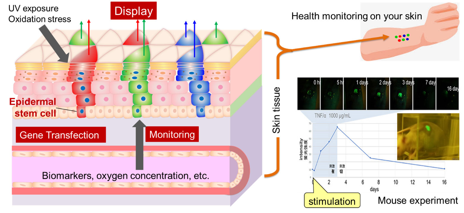
Another recent research theme is the “skin display,” which turns the skin itself into a living sensor and display. The skin constantly produces new cells and sheds old ones as dead skin. By focusing on epidermal stem cells that support this regeneration, researchers designed artificial skin to produce fluorescent proteins in response to internal signals such as inflammation. When this artificial skin is transplanted, part of the skin glows according to changes in physical condition. Experiments using mice confirmed that the glow became stronger when an inflammatory stimulus was applied, returned to normal when the stimulus subsided, and reacted again when the stimulus was applied once more. Specially Appointed Professor Fujita describes this mechanism as something like a mole. Wearable sensors that resemble adhesive bandages require reapplication and power sources. Living cells embedded in the skin, however, may remain in the same place and continue working together with the body. By changing the signals to be detected, it may be possible to use color differences to indicate changes in physical condition, such as oxygen deficiency or heatstroke, in addition to inflammation. Applications are envisioned not only for humans, but also for pets and livestock that cannot communicate poor health in words.
From MEMS to light, to energy, to cells, and then to living skin, Specially Appointed Professor Fujita’s research has expanded by connecting different fields. One factor behind this development is more than 30 years of joint research with France. In the 1990s, a French research institution began looking for a micromachine research partner in Japan, which led to collaboration with the Institute of Industrial Science at the University of Tokyo. Since then, several hundred researchers have stayed in Japan, and researchers from Japan and France have brought together their respective strengths. This long-running collaboration has continued for more than 30 years because the two sides built a deep relationship of trust and established a complementary relationship rather than a competitive one.
Specially Appointed Professor Fujita first encountered micromachines in 1986, after working on a number of topics including nondestructive testing and autonomous distributed systems at the University of Tokyo, as well as superconducting magnet research at MIT. A senior researcher recommended the new field of micromachines, and Fujita became interested in the idea of creating machines through semiconductor technology. Ideas do not easily emerge when one looks only within one’s own specialty. They arise when listening to talks from other fields at international conferences, when encountering lectures by collaborators, or when thoughts circulate during sleepless nights caused by jet lag. New seeds of research are born when information coming from outside connects with one’s own sense of problems. Specially Appointed Professor Fujita compares research to surfing. Places where everyone gathers quickly become crowded. But if you can find a good place early and catch the wave, the larger movement that comes afterward will push you forward. To do that, it is necessary to accumulate knowledge, keep one’s antenna up, and maintain a sense of inquiry. Research and development, he says, can also be compared to mountain climbing. You choose the right summit to climb. You thoroughly investigate the route that will take you there. You make one decision after another about how to overcome difficult points along the way. “Research themes themselves become old as times change, but I think research methods remain the same. They say the god of opportunity has hair only at the front. What matters is to keep thinking and stay prepared, so that when that forelock comes by, you can grab it.”
Specially Appointed Professor Fujita sees engineering not merely as useful technology, but as culture. Just as Edo-period karakuri mechanical dolls are both technology and cultural assets, research also has universal value. One of his favorite paintings is René Magritte’s The Empire of Light. In it, a daytime sky and nighttime ground, things that ordinarily do not exist at the same time, meet within a single painting. Machines and semiconductors. Light and structures. Cells and sensors. When unlike things meet, sparks are created, and new questions arise there. “We must try to see not what already exists, but what does not yet exist. Good research depends on how good a question you can ask.”
The sensors that measure orientation inside smartphones, the tiny mirrors that read what lies ahead of cars, the elements that extract electricity from the vibrations of factory equipment, the tweezers that measure cell stiffness, and the skin that uses light to show changes in physical condition are all technologies that extract invisible information and convert it into forms people can understand. Microscopic machines are not merely small. They enter the space between the invisible world and human society, illuminating, moving, measuring, and notifying. Specially Appointed Professor Fujita’s research began with tiny structures fabricated on semiconductors, and has now expanded into living cells. To see what is still unseen, tiny machines continue to move quietly today.
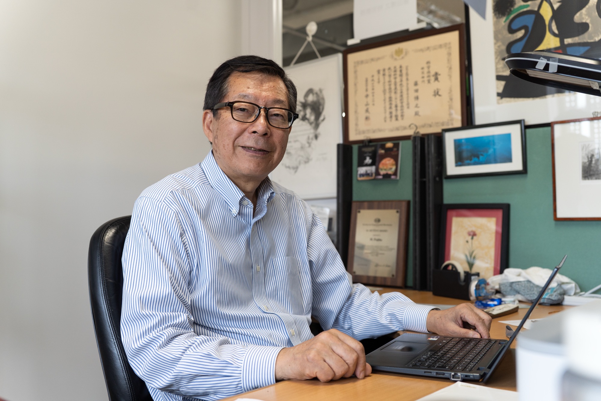
Specially Appointed Professor, Micro-nano Systems Laboratory, Advanced Research Laboratories, Tokyo City University. In 1980, he completed the doctoral program in electrical engineering at the Graduate School of Engineering, The University of Tokyo, and received a Doctor of Engineering degree. After serving as Professor at the Institute of Industrial Science, The University of Tokyo; Director of the Center for International Research on MicroMechatronics (CIRMM); and Director of the Advanced Research Laboratory at Canon Medical Systems Corporation, he assumed his current position in 2018.